Hardware and operating systems · part 2 of 3
SRAM, DRAM and storage: how each technology stores a bit
How SRAM, DRAM, flash and disk store a bit inside, why SRAM is fast and expensive, why DRAM is slow and cheap, and what keeps data after power loss.
intermediatePublished on · 41 min read
Think of two classmates who are always arguing. One claims the opposite of whatever the other just said, and the fight repeats forever, because each one demands the right answer from the other. That is the idea behind the pair of inverters in a loop from the lesson on sequential circuits, and it is how SRAM stores a bit: the answer lives as long as the loop stays powered. If the power goes out, the argument stops and the answer disappears.
DRAM is more like a bucket with a hole. The bit is the water, the hole lets it drain, and someone has to refill the bucket before it runs dry. Flash stores the bit like a message locked in an envelope inside another envelope: the charge stays trapped there without anything being powered. The magnetic disk is an LP record. To play a track, the needle has to reach the right groove, and the music only starts when the point you want passes underneath it.
This lesson explains why these four technologies cost and behave so differently, and why SRAM is fast and expensive while DRAM is slow and cheap. It assumes the two-inverter loop and the latch from the lesson on sequential circuits, and the lesson on the memory hierarchy and locality, which showed why there are several levels and where each one fits. The hierarchy will not be repeated here. We will look inside the cells, which is where the price comes from.
Two terms appear right away. A bit is a stored value of 0 or 1. A cell is the smallest piece of a memory chip that stores one bit. Volatile memory loses its content when the power is gone, and non-volatile memory keeps it without power. The other terms are defined when they first appear, and the glossary at the end gathers them all.
Lesson map
| Section | Question it answers |
|---|---|
| 1. What each technology is | What are the four families, and what separates them? |
| 2. What it is for | Why does the same acronym, RAM, cover memories with such different costs? |
| 3. Examples in different contexts | Where does each family show up in everyday use? |
| 4. How it works inside | How does each cell store, read, lose and recover the bit? |
| 5. Details and edge cases | Which variants and limits exist? |
| 6. Common mistakes and good practices | Which misconceptions appear when using these memories? |
| 7. The program that checks the numbers | How can the numbers in this lesson be reproduced? |
| 8. Exercises | How can you practice, with reference answers? |
| 9. Glossary | Which terms does the lesson use? |
| What was not confirmed | What lacks a primary source or a measurement? |
| Sources | Where do the facts come from, and when were they consulted? |
1. What each technology is
There are four families that matter in this lesson. SRAM is the cache memory: fast and expensive per bit. DRAM is the main memory of the computer: slower and cheaper. Flash is what you find in USB drives, memory cards and SSDs, and it keeps the bit without power. The magnetic disk is the traditional hard drive, which also keeps the bit without power, but with parts that move. The first two are volatile. The last two are not.
Why separate volatile from non-volatile right at the start? Because this difference decides how each one gets used. No program keeps its variables only on a USB drive, because the drive is too slow to keep up with the CPU. At the same time, nobody keeps family photos only in RAM, because they would vanish when the computer is turned off. Each family has its place because it combines one type of physics with one type of use.
The cost also has a physical origin. Each family stores the bit with a different phenomenon: a loop of transistors that holds itself, a charge on a capacitor that leaks away, a charge trapped in an isolated gate, a magnetic orientation that follows the platter. The more parts a bit needs, and the less it holds on its own, the more expensive the bit becomes, or the more care the circuit around it must take.
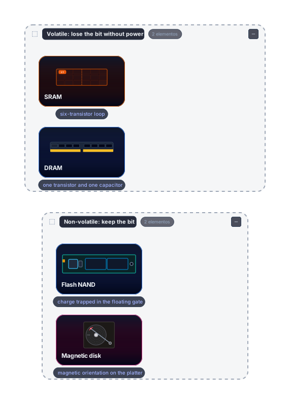
The figure separates the families by whether they lose or keep the bit without power. The groups on the left are volatile, and the ones on the right are not. Each card shows an icon for the physical part and the sentence that describes how the bit is stored. The icons only identify each family, and they do not indicate size or price. The lesson did not measure price or access time in this figure. Timing numbers appear in section 4.10, with the reference CPU and the sources.
2. What it is for
The CPU needs bits that answer in a few cycles when they are nearby, many bits farther away at a reasonable price, and bits that survive a shutdown. No single technology meets all three requirements, which is why the hierarchy from the lesson on the memory hierarchy and locality exists. One question the hierarchy does not answer on its own: why do SRAM and DRAM have such different costs, if both are called RAM?
RAM stands for random access memory. The acronym describes the access pattern, which lets you read any address in about the same time, and not the physics of the cell. That is why it covers two different things. SRAM uses a six-transistor loop per bit, and the loop only works while there is power. DRAM uses one transistor and one capacitor per bit, and the capacitor loses charge over time. The first spends parts so it does not need maintenance. The second saves parts and pays with constant maintenance, the refresh described in section 4.5.
Flash and disk enter because the question changes. For someone who wants to keep a photo for years, what matters is whether the bit is still there after shutdown, and how much each gigabyte costs. That is why the lesson covers all four together, with one reading rule: the first two concern a bit that lives while there is power, and the last two concern persistence.
3. Examples in different contexts
The first example is the cache of a core. A modern processor keeps in SRAM the data it has just used, because the CPU waits extra cycles for every access that misses. With the reference CPU of this lesson (section 4.10), the L1 cache responds in 4 cycles. In this case, paying six transistors per bit is worth it, because the time gained matters more than the space lost on the chip.
The second example is the memory of a notebook. Running programs live in DRAM, in a quantity much larger than the cache. When the notebook is turned off, that content disappears, so whatever must survive a shutdown has to be written to non-volatile storage. DRAM is cheap per bit because each bit uses one transistor and one capacitor, not a whole loop.
The third example is the USB drive. You save a photo on it, pull the drive out of the port, and the photo is still there. The flash cell traps the charge in an isolated gate, and that charge does not need power to stay trapped. The drive, however, writes in pages and erases in blocks, so replacing one photo with another takes more work than it seems. Section 4.8 explains that work.
The fourth example is a backup disk, which stores many gigabytes for little money. To read one large file in a single pass, the disk does well. To read many small files scattered across the platter, the story changes, because the arm has to travel to each track and wait for the sector to pass. Section 4.9 does that calculation.
The four cases show that the cost per bit and the access speed appear together, but the math changes with the usage pattern. A cache deals with few bits and accesses in a row. A backup disk deals with volume. Looking at the usage pattern before looking at the price table already decides much of the choice.
4. How it works inside
This section opens each memory down to the transistor. The circuit figures use block symbols, because ArchFlow has no transistor element. Each ci in the figure is a three-pin transistor: the gate on the left, and the drain and source on the right. That is the drawing’s convention, and the section “What was not confirmed” repeats this caveat.
4.1 The SRAM cell: six transistors in a loop
An SRAM cell has six transistors. Drepper writes that a cell requires six transistors and that variants exist, and Mason’s note from Michigan State University describes the cell with two access transistors and its hold, write and read operations. Four of the transistors form two inverters wired in a ring, exactly like the loop in the lesson on sequential circuits. Each inverter is a pair of complementary transistors: a PMOS that connects the output to the supply, and an NMOS that connects it to ground, as seen in the lesson on the transistor as a switch. The other two are the access transistors, which section 4.2 presents.

The figure shows only the core, so that the feedback stays visible without the access transistors mixed in. The supply VDD reaches the top terminal of each PMOS, and each NMOS goes down to ground. The two inverters have their gates connected to one input node, and their outputs connect to the opposite node. Follow the path of the bit: the drain of P1 and the drain of N1 form node Q, which carries the value to the gates of P2 and N2. The output of P2 and N2 forms node Qn, which comes back over the top and enters the gates of P1 and N1. The labels on the boxes give the value of each input: with Q at 1, the gate of P2 sees 1 and turns the PMOS off, while the NMOS of N2 conducts and pulls Qn to 0. That 0 returns to the gates of P1 and N1 and confirms the state. Neither inverter decides alone. The answer lives in the whole circuit, which is the idea the lesson 2.3 showed with the latch.
4.2 Access and read: the word line and the bit pair
The core alone holds the value, but it cannot be read or written from outside. Two access transistors, M5 and M6, handle that, connecting the nodes Q and Qn to the bit lines BL and BLn. The word line, WL, controls both transistors at once. When WL is 0, the accesses are cut off and the core isolates itself from the rest of the chip. When WL rises, the accesses conduct, and the value can be read or written through the pair of lines.

The figure shows the retention state, with WL at 0 V. Accesses M5 and M6 are off, and the core, represented by the block with outputs q and qn, neither receives nor sends anything over the lines. The two bit lines appear at 1 V, which is the precharge level the lesson adopts. The word line reaches the gates of M5 and M6 through the same wire, and each of the two core outputs connects to one drain or source of an access transistor. On a read, WL rises and both accesses conduct, as figure 04 shows.
To read, the word line rises and the cell starts to act on the bit lines. Figure 04 follows the sequence. With Q equal to 1, the side that stores 0 is Qn. It pulls the line BLn down through the path that goes through the inverter. The BL line, on the side that stores 1, stays high. A read amplifier compares the two lines and decides the value from the difference between them, without waiting for either one to reach its final value.
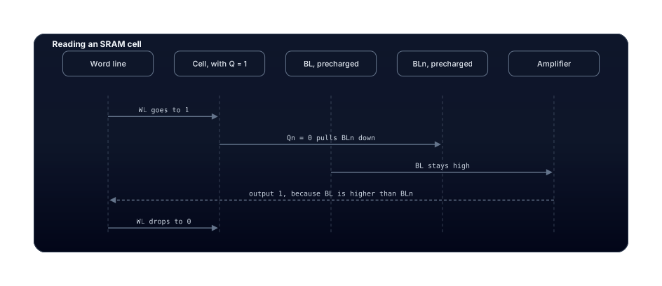
The sequence has one rule: both lines start equal, and the cell creates the difference. Read the message in which Qn equal to 0 pulls BLn down, while BL stays high because Q is 1. The amplifier only needs to see that BL is larger than BLn. The last message closes the sequence with the word line dropping, and the core holds the value on its own again. Why is this read fast? Because the cell itself drives the bit line with transistors, without depending on a capacitor that shares its charge with the line. That is the contrast section 4.3 draws with DRAM. The cost of the fast path shows up in the silicon: six transistors per bit, and a loop that needs power to keep existing.
4.3 The DRAM cell: one transistor and one capacitor
DRAM replaces the loop with a much simpler part. A capacitor stores electric charge, and the presence or absence of charge represents the bit. A single access transistor connects the capacitor to the bit line when the word line rises. Drepper summarizes the structure in one sentence: one transistor and one capacitor, where the capacitor stores the state and the transistor guards access to it. MSU’s note says the same thing in other words: an nFET for access, a storage capacitor, and the word line as the control.

The figure has a transistor M, the capacitor Cs that stores the bit with Vs = 1 V, and the bit line capacitance, Cbit, connected to ground. The word line WL is at 0 V, so M is off and the charge in Cs does not leave. When WL rises, M conducts, and Cs starts to share its charge with the line. The amplifier, drawn as a voltmeter, represents in simplified form the read circuit from section 4.2. In DRAM, the bit line works as a capacitance that receives the charge of Cs, so the variation the amplifier sees is small.
This simplicity has a direct effect on the price. Drepper says the DRAM cell is many times smaller than the SRAM cell, so more bits fit in the same silicon area. The price of this economy shows up in reading and maintenance, which sections 4.4 and 4.5 explain.
4.4 The read that erases and the write-back
When Cs shares its charge with the bit line, the voltage of Cs changes, and the original value stops existing in the cell. MSU’s note is direct: a DRAM read is destructive, and the operation must include a simultaneous write-back. Drepper describes the same phenomenon with other vocabulary: the read consumes the capacitor’s charge, and the amplifier’s output is sent back to the capacitor to recharge it.
The charge-sharing math is in MSU’s note. The initial charge of Cs, Vs times Cs, is redistributed between Cs and Cbit until a final voltage, Vf = Cs · Vs / (Cs + Cbit). With Cbit ten times larger than Cs, a value chosen only for the example, the final voltage is Vs / 11, about 9% of Vs. The note itself says this voltage is very small and requires a good read amplifier. Reading DRAM, therefore, means noticing a small difference while, at the same time, emptying the source of the information.
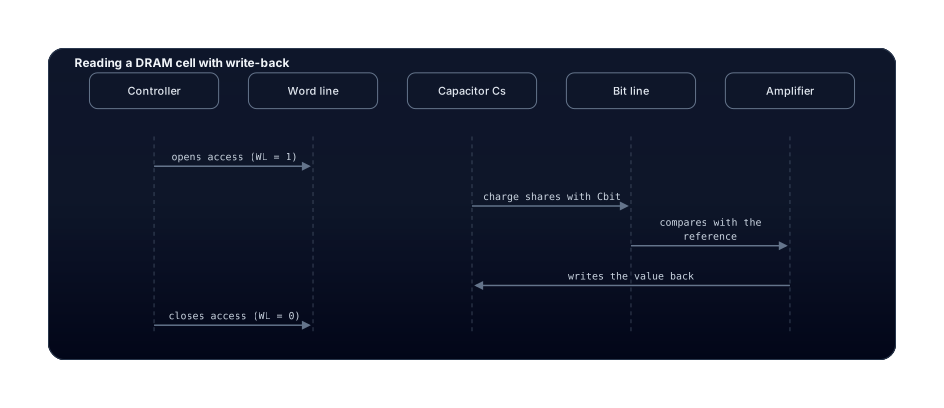
The sequence has five steps, read from top to bottom. The controller opens the access by raising WL. Next, the charge of Cs shares with the bit line. The amplifier compares the line with the reference and decides the value. The write-back returns that value to Cs, and finally the controller closes the access by lowering WL. The fourth step is what keeps the read from erasing the bit, because the read spent the charge and the write-back returns it. This step has a cost. Drepper says that reading needs extra time and energy because of the write-back. Without the write-back, the value read would leave the memory, and the data itself would be lost.
4.5 Refresh: the bucket that must be refilled
The capacitor does not hold its charge forever. Even with the access transistor off, the charge drains through a leakage current, which Drepper calls leakage, and the bit is lost over time. That is why DRAM needs a periodic update, the refresh.
Refresh is a read followed by a write-back, in which the value read is discarded, and it must reach every row within a time window. Drepper states that, for most DRAM chips of that time, the window was 64 ms, according to the JEDEC specification. To make the arithmetic visible, he gives an example: with 8192 rows, the controller issues a refresh command, on average, every 7.8125 µs. During a refresh cycle, memory access is not possible, and Drepper cites a study according to which, in some workloads, this overhead can stall up to 50% of the accesses.
For DDR5 memories, Wikipedia states that the window drops to 32 ms up to 85 °C and to 16 ms between 85 °C and 95 °C. This value was not checked against the JEDEC text in this lesson, and the confirmation section says so.
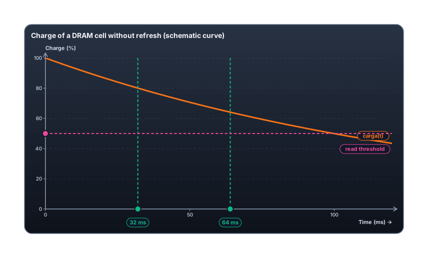
The curve is an exponential chosen to show the decay, and it was not measured on any chip. The constant of 144 ms was chosen for the drawing. With it, the charge falls to about 80% of the initial value at 32 ms, and to about 64% at 64 ms. It crosses the 50% threshold near 99.8 ms, which is 144 · ln 2. That instant does not belong to a real chip. The figure shows only the loss: refresh does not appear in it, and it is refresh that would bring the charge back to its initial level in every window. For refresh to work, the charge has to be above the threshold at the end of each window, and the marks at 32 and 64 ms show where those windows fall.
4.6 SRAM and DRAM side by side, and the cost per bit calculation
After the mechanisms, the comparison fits in a table. Each row is explained in the earlier sections.
| Characteristic | SRAM | DRAM |
|---|---|---|
| Parts per bit | Six transistors | One transistor and one capacitor |
| Read | Direct: the cell drives the bit line | Destructive: requires a write-back |
| Refresh | Not needed | Required. 64 ms window in Drepper’s example, and 32 ms in DDR5 according to Wikipedia |
| Density | Lower | Higher: cell many times smaller, according to Drepper |
| Cost per bit | Higher | Lower, according to MSU’s note |
| Typical use in this track | Cache | Main memory |
The table calls for a calculation. A memory’s cost has several parts, such as silicon, the manufacturing process, packaging and sales volume, and the lesson has no market price for any of them. But the part that depends only on the cell’s architecture can be counted. Counting parts per bit is a sound first approximation: it does not give the price, but it does show how much silicon each bit requires. For 1 GiB, there are 8 × 2³⁰ bits, about 8.59 × 10⁹ bits. In SRAM, that gives 6 × 8.59 × 10⁹, about 5.15 × 10¹⁰ transistors. In DRAM, it gives 8.59 × 10⁹ transistors and the same number of capacitors. The transistor ratio is 6 to 1, and section 7 reproduces the number with the program. The DRAM capacitor, however, is a different structure from the transistor, and the lesson does not compare areas in square micrometers. So the calculation says how many parts exist, not how much each one costs.
A quick reading of the table: SRAM trades parts for speed, and DRAM trades maintenance for density.
4.7 Flash: charge trapped in an isolated gate
The flash cell starts from a common MOSFET with an extra gate. This extra gate is called the floating gate, because it has no electrical connection to anything, and it is isolated by a layer of oxide. According to Wikipedia, electrons placed on it stay trapped, because the insulating layer surrounds them. The trapped charge blocks part of the electric field of the control gate, and Wikipedia says this raises the threshold voltage, VT, at which the transistor conducts. That difference is what the read detects: an intermediate voltage on the control gate makes the transistor conduct or not, depending on the trapped charge.
The charge stays there without power, and that is the persistence of flash. What the lesson did not confirm is how many years it lasts, because no primary source on that was read. The confirmation section says what was checked.

A flash cell rarely appears alone. Wikipedia describes the NAND organization as a chain: the source of one cell connects to the drain of the next, and cells connected in series form a string. The figure draws four cells, C0 to C3, each with its own word line, WL0 to WL3, on its gate. To read C2, the word line WL2 goes to 0 V, the read level of the chosen cell. The other words receive a pass voltage, which makes the neighboring cells conduct without depending on their own bit. The current therefore crosses the whole chain and reaches the bit line, and the value of C2 controls the passage. The selection transistors at the ends, which complete the chain, are not drawn. The figure is a simplified chain, and the section “What was not confirmed” says what was left out.
4.8 Pages, blocks and the write to another page
A NAND string is organized in pages, and the pages in blocks. According to Wikipedia, reading and programming happen per page, with typical pages of 4 KiB to 16 KiB. Erasing happens on the whole block, which gathers several pages. This asymmetry has a direct consequence: a page that already holds data cannot be rewritten in the same place. The new content goes to a free page, the old one is marked invalid, and the block is only reused after being erased as a whole.
The difference from NOR matters too. Wikipedia says NOR offers a full address bus and random access, which serves to run code directly from memory. NAND has no external random address bus, and its data is read in pages. This is why NAND serves for mass storage.
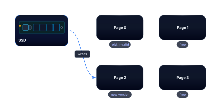
The figure shows the most common case. The SSD receives the new version of some data. Page 0 holds the old version, which is now invalid and appears with the error state. The new version goes to page 2, which was free. Pages 1 and 3 remain free, and the block is not erased on this write. When the free pages run out, the controller must copy the valid pages to another block and erase the old one, and that erase is the cost discussed in error 3 of section 6. The figure does not show the controller or the channels, because the lesson did not confirm the architecture of a real SSD.
4.9 Magnetic disk: seek, wait and transfer
The disk stores bits as magnetic orientation on a spinning platter, and a read head sits over it at the tip of an arm. To read a random sector, three times add up. First, the arm moves the head to the right track: this is the seek. Then the head waits for the desired sector to pass underneath it: this is the rotational latency. Finally, the sector is transferred.
The average rotational latency is half a turn of the platter. At 7,200 rpm, one turn lasts 60,000 ms divided by 7,200, about 8.33 ms, and half a turn gives 4.17 ms. Wikipedia has this same line in a table of HDD performance, which confirms the calculation. The average seek of 8.5 ms comes from an old Seagate datasheet for a BarraCuda 7200.7 model, copied on a manuals website, and the original datasheet was not opened in this query. Wikipedia gives about 9 ms for desktop drives without citing a source. With 9 ms, the random access takes 13.17 ms, and the conclusion of section 4.10 does not change.
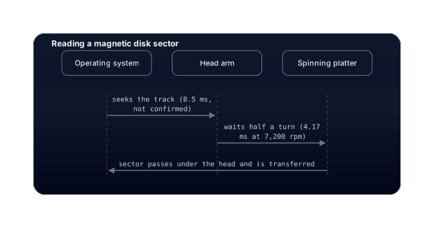
The sequence has one rule: the arm moves on every random sector, and the platter keeps spinning during the seek. The figure shows the three waits in order. The 8.5 ms seek is marked as not confirmed, and the half turn of 4.17 ms comes from the calculation at 7,200 rpm. The transfer of the sector appears as the last message, but it does not enter the calculation in section 4.10, because the lesson did not measure the transfer rate. The sum of the two waits is a simple model. It assumes that the right sector arrives at a random position when the arm finishes the seek.
4.10 The numbers of a reference CPU
The numbers in this lesson use the same reference CPU as the lesson on the memory hierarchy and locality: a Zen 4 core converted to 4.0 GHz, where each cycle lasts 0.25 ns. The Chips and Cheese article about the Ryzen Z1, dated February 12, 2024, gives the core latencies: L1 of 4 cycles, L2 of 14 cycles and L3 a little above 50 cycles. For main memory, the same article gives 123.9 ns on the Z1, which uses LPDDR5, a memory used in portable devices and not the DDR5 DRAM of a desktop.
The conversion to nanoseconds depends on the clock, and the article does not report the clock of the test. That is why the 4.0 GHz is a convention of this lesson, not a measurement. The difference appears in the article itself: the Z1’s L3 is given as 14.16 ns, and that of desktop Zen 4 cores as 10.46 ns. With the 4.0 GHz convention, 50 cycles become 12.5 ns, and the Z1’s L3 would correspond to about 57 cycles. The table below uses the convention, and the confirmation section shows the range.
| Level or operation | Cycles at 4.0 GHz | Time | Status |
|---|---|---|---|
| L1 (SRAM) | 4 | 1 ns | Measured in the article, in cycles |
| L2 (SRAM) | 14 | 3.5 ns | Measured in the article, in cycles |
| L3 (SRAM) | about 50 | 12.5 ns | Measured in the article, in cycles |
| DRAM (Z1, LPDDR5) | about 496 | 123.9 ns | Measured in the article, in ns |
| NVMe SSD | about 60,000 | 15 µs | Not confirmed |
| Disk: 8.5 ms seek plus half a turn | about 50.7 million | 12.67 ms | Seek not confirmed, half turn calculated |
With this scale, a random disk access costs about a million times one L3 hit. The exact figure comes from the program in section 7, which gives the ratio of 1.01 × 10⁶. The same number appears in the table and in figure 10, and both come from the same calculation. The DRAM latency in the table is that of the Z1, and the cache lesson, not written yet, will need another measurement before this value can be generalized.
5. Details and edge cases
SRAM and DRAM lose the data when the power drops, and that is what makes them volatile. The difference between them appears while the power is on. SRAM keeps the bit without any update, because the loop sustains itself. DRAM needs the refresh from section 4.5 all the time, even with the computer on and idle.
Drepper mentions variants of the six-transistor cell, without detailing them in the excerpt consulted. The lesson did not measure any of them.
Flash has a weakness that DRAM does not have: wear. Wikipedia says flash has a finite number of program and erase cycles, abbreviated P/E, and that erasing a cell becomes slower with use. The SSD controller tries to spread the writes so that no block wears out before the others, but this practice was not confirmed by a source in this lesson. What the lesson confirms is the physical rule: the cell does not tolerate infinite switching.
NOR and NAND are told apart by the type of access. NOR serves to execute code, because it has a full address bus. NAND serves to store a lot of information, because it reads in pages. Section 4.8 focuses on NAND because it is the organization the lesson describes for mass storage.
The magnetic disk has a detail that the calculation in section 4.9 exposes. When the sectors read are in sequence, the arm barely moves, and the wait is limited to rotation. When the sectors are scattered, each read pays for a new seek. It is the same locality idea from lesson 4.1, applied to a mechanical medium.
6. Common mistakes and good practices
Mistake 1: thinking that an SSD and RAM are the same thing with different prices. Anyone who has lost a file that existed only in memory has learned the difference without needing a table. RAM is volatile, and the SSD is non-volatile. RAM responds in cycles, and the SSD responds in microseconds. Good practice: decide what must survive a shutdown before deciding where the data lives.
Mistake 2: thinking that DRAM holds the bit by itself, like a register. DRAM depends on the controller’s refresh, and a DRAM that stopped being refreshed would lose its data. Good practice: when looking at main memory, think of it as a continuous service, which consumes time and energy just to keep being memory.
Mistake 3: thinking that rewriting a page only touches that page. According to section 4.8, rewriting a page with data means placing the new content in another free page and, when there are no free pages left, copying what is valid and erasing a whole block. Good practice: group small writes into larger blocks, so that the cost of copying and erasing spreads over more data. The lesson did not measure this gain, but the calculation comes from the physics itself.
Mistake 4: measuring a disk by its transfer rate and concluding that it is fast. The rate applies to sequential reads. In random access, the seek and the rotational wait dominate the calculation, as section 4.9 shows with 12.67 ms. Good practice: read data in sequence whenever the program allows it, and remember that this is the spatial locality from lesson 4.1 in another medium.
Mistake 5: treating SRAM as the faster memory because it is more expensive. The price comes from the cell’s design. The speed comes from the read mechanism: the six-transistor loop is fast because the cell itself drives the bit line. Good practice: compare memories by their read mechanism, not by their price tag.
Mistake 6: using the number of transistors per bit as a price. The count in section 4.6 shows how much silicon each bit requires, not how much it costs. Price also depends on process, yield and volume, and none of these entered the calculation. Good practice: use the count to compare architectures, and look for the price in a market source before making a purchase decision.
7. The program that checks the numbers
The program below repeats the calculations of this lesson with the 4.0 GHz convention and with the values from the sources. It does not simulate the circuit. It only checks the arithmetic, so that no number in the lesson depends on a calculation done in your head. The transistor count per GiB was added in this revision and appears in section 4.6. The labels in the program and in its output stay in Portuguese, as in the original lesson.
# Contas da aula 4.2 com a CPU de referência: núcleo Zen 4, convertido a 4,0 GHz.
clock_hz = 4.0e9
ciclo_ns = 1e9 / clock_hz
print(f"ciclo a 4,0 GHz: {ciclo_ns:.2f} ns")

# Refresh: 8192 linhas, janela de 64 ms, um comando por linha por janela
linhas = 8192
janela_ms = 64
intervalo_us = janela_ms * 1000 / linhas
comandos_por_s = linhas / (janela_ms / 1000)
print(f"intervalo entre comandos de refresh: {intervalo_us:.4f} us")
print(f"comandos de refresh por segundo: {comandos_por_s:.0f}")

# Disco a 7200 rpm, busca média de 8,5 ms (ficha antiga, não confirmada)
rpm = 7200
meia_volta_ms = 60_000 / rpm / 2
busca_ms = 8.5
acesso_ms = busca_ms + meia_volta_ms
print(f"meia volta a 7200 rpm: {meia_volta_ms:.2f} ms")
print(f"busca mais espera de meia volta: {acesso_ms:.2f} ms")

# Comparação com o L3 de 50 ciclos
l3_ns = 50 * ciclo_ns
print(f"L3 de 50 ciclos: {l3_ns:.1f} ns")
print(f"disco em ciclos: {acesso_ms * 1e6 / ciclo_ns:.2e}")
print(f"vezes mais lento que o L3: {acesso_ms * 1e6 / l3_ns:.2e}")

# Compartilhamento de carga, modelo simplificado da MSU, com Cbit = 10 Cs
Cs, Cbit, Vs = 1.0, 10.0, 1.0
Vf = Cs * Vs / (Cs + Cbit)
print(f"tensão final na linha de bit (Cbit = 10 Cs, Vs = 1): {Vf:.4f} = Vs / 11")

# Transistores e capacitores por byte e por GiB
bits_por_byte = 8
bits_gib = 8 * 2**30
print(f"1 byte em SRAM 6T: {bits_por_byte * 6} transistores")
print(f"1 byte em DRAM 1T1C: {bits_por_byte} transistores e {bits_por_byte} capacitores")
sram_gib = bits_gib * 6
dram_gib = bits_gib
print(f"1 GiB em SRAM 6T: {sram_gib:.3e} transistores")
print(f"1 GiB em DRAM 1T1C: {dram_gib:.3e} transistores e {dram_gib:.3e} capacitores")
print(f"razão de transistores SRAM/DRAM: {sram_gib / dram_gib:.0f}")
The program was run with python3 -I contas.py, in isolated mode, and this is the real output:
ciclo a 4,0 GHz: 0.25 ns
intervalo entre comandos de refresh: 7.8125 us
comandos de refresh por segundo: 128000
meia volta a 7200 rpm: 4.17 ms
busca mais espera de meia volta: 12.67 ms
L3 de 50 ciclos: 12.5 ns
disco em ciclos: 5.07e+07
vezes mais lento que o L3: 1.01e+06
tensão final na linha de bit (Cbit = 10 Cs, Vs = 1): 0.0909 = Vs / 11
1 byte em SRAM 6T: 48 transistores
1 byte em DRAM 1T1C: 8 transistores e 8 capacitores
1 GiB em SRAM 6T: 5.154e+10 transistores
1 GiB em DRAM 1T1C: 8.590e+09 transistores e 8.590e+09 capacitores
razão de transistores SRAM/DRAM: 6
The output matches the text: the cycle of 0.25 ns, the refresh every 7.8125 µs, the disk at 12.67 ms, the ratio of about one million, and the ratio of 6 in transistors per GiB. The value 0.0909 is the fraction from the simplified model, and it is not a measurement of a chip.
8. Exercises
- A byte is stored in six-transistor SRAM and, in another chip, in one-transistor, one-capacitor DRAM. How many transistors does each one use for that byte, and how many capacitors does the DRAM use?
Answer: the SRAM uses 8 × 6 = 48 transistors. The DRAM uses 8 transistors and 8 capacitors. The calculation is the same line as the program in section 7.
- A DRAM chip has 8192 rows and a refresh window of 64 ms. What is the average interval between two refresh commands, and how many commands are issued per second, assuming one command per row in each window?
Answer: 64 ms divided by 8192 gives 7.8125 µs. Since there are 8192 commands in every 64 ms, 128,000 commands are issued per second. The assumption of one command per row is Drepper’s example, not the specification of a current chip.
- A disk at 7,200 rpm has an average seek of 8.5 ms. How long does a random access take when it waits half a turn, and how many times slower is it than an L3 hit of 50 cycles at 4.0 GHz?
Answer: 8.5 ms plus 4.17 ms gives 12.67 ms. The L3 of 50 cycles at 4.0 GHz takes 12.5 ns. The ratio is about 1.01 million. The result depends on the 8.5 ms seek, which comes from an old datasheet and is marked as not confirmed. With the 9 ms seek that Wikipedia cites without a source, the access rises to 13.17 ms, and the ratio to about 1.05 million.
- Why does an SSD not rewrite a page in the same place?
Answer: a page is only programmed after the block that contains it has been erased. Since erasing happens on the whole block, rewriting a page with data requires placing the new content in another free page and marking the old one as invalid. When there is no free page, the valid data must be copied and the whole block erased first. That is why the rewrite has a copying cost and, sometimes, an erasing cost.
- Why does a DRAM read need to be followed by a write-back?
Answer: the read shares the capacitor’s charge with the bit line, and that empties the capacitor. The output of the read amplifier is sent back to the capacitor to recharge it. Without this write-back, the value read would not stay stored in the cell.
- In the SRAM core, Q is 1. What is Qn, and why?
Answer: Qn is 0. The gates of P2 and N2 receive Q equal to 1: the PMOS turns off and the NMOS conducts, pulling Qn to 0. That 0 reaches the gates of P1 and N1, which keep Q at 1. Both sides of the loop are consistent, and that is why the state holds.
- An SRAM chip and a DRAM chip both have a capacity of 1 GiB, and the lesson counts only transistors. How many transistors does each chip have, and how many capacitors does the DRAM have? Why is this count not enough to tell which of the two costs more?
Answer: the SRAM has 6 × 2³³ bits, about 5.15 × 10¹⁰ transistors. The DRAM has 2³³ bits, about 8.59 × 10⁹ transistors and the same number of capacitors. The calculation shows that SRAM requires six times more transistors. It is not enough to tell the cost, because the price also depends on the area of each structure, the manufacturing process, the yield and the volume. The lesson does not have these data.
9. Glossary
Bit: the smallest amount of information, a value of 0 or 1.
Cell: the smallest part of a memory chip that stores one bit.
Volatile: memory that loses its content when the power goes away.
Non-volatile: memory that keeps its content without power.
SRAM: static memory made of transistor loops, fast and expensive per bit, which needs no refresh while powered.
DRAM: dynamic memory made of one transistor and one capacitor per bit, cheaper and denser, which needs refresh.
Capacitor: component that stores electric charge, and the part that holds the bit in DRAM.
Access transistor: transistor that connects a cell to the bit line when the word line is active.
Word line (WL): wire that controls the access transistors of a row of cells.
Bit line (BL and BLn): wires through which the bit is read and written. BLn is the complementary line of BL.
Precharge: setting the bit lines to a known level before a read.
Sense amplifier: circuit that compares the two bit lines and decides the value from the difference between them.
Destructive read: a read that changes the content of the cell, as in DRAM, and therefore requires a write-back.
Refresh: a read followed by a write-back, performed periodically to restore the charge that leaks from the capacitor.
Retention: the time a cell keeps its bit without an update.
Read threshold: the charge or voltage level below which the circuit reads the other value.
Floating gate: the isolated gate of a flash transistor, with no electrical connection, where electrons stay trapped.
Pass voltage: voltage applied to the unread words of a NAND string, so that the neighboring cells conduct.
NAND: a type of flash organized in chains, read and written in pages and erased in blocks.
NOR: a type of flash with a full address bus, which allows random access to each byte.
Page: the smallest unit of reading and programming in NAND.
Block: the smallest erase unit in NAND, made of several pages.
Controller: the SSD circuit that receives the system’s requests and distributes them across the chips.
Seek: movement of the disk arm to the desired track.
Rotational latency: the wait until the desired sector passes under the read head.
RPM: revolutions per minute of the disk platter.
What was not confirmed
The timing numbers in this lesson come from a primary source, the Chips and Cheese article itself, and from calculations the text indicates. Even so, there are gaps that must be stated clearly.
The reference CPU uses 4.0 GHz as a convention, because the Chips and Cheese article does not report the clock of the test. The same article gives 14.16 ns of L3 on the Z1 and 10.46 ns for desktop Zen 4 cores. At 4.0 GHz, these values are equivalent to about 57 and 42 cycles. The cycles in the table in section 4.10 hold under the convention, not for a measured clock.
The average seek of 8.5 ms comes from the datasheet of an old model, the BarraCuda 7200.7, copied on a manuals website. The original Seagate datasheet returned error 403 in this query, and no current model was verified. Wikipedia gives about 9 ms for desktop drives, without a citation. The 4.17 ms half turn is a calculation from 7,200 rpm, and the sum of the two waits is a model: it assumes that the right sector arrives at a random position at the end of the seek.
The read latency of a NAND page and of a whole SSD was not confirmed. The lesson cites no datasheet figure for it. Lesson 4.1 gives 15 µs for an NVMe SSD, and this value was not verified here either.
The 123.9 ns DRAM latency belongs to the Z1, with LPDDR5, and not to a desktop DDR5 DRAM. The lesson has no other measurement of desktop DRAM with a primary source in this query. The range of 60 to 90 ns that appeared in earlier versions of lesson 4.1 has no source and does not enter this lesson.
The values of 32 ms and 16 ms for DDR5 come from Wikipedia and were not checked against the JEDEC text. A tREFI value of 3.9 µs appeared in a search result, citing a Micron note, but that note was not read, so the value does not enter the text as fact. The example of 8192 rows and 7.8125 µs describes the organization of a chip from the period of Drepper’s text, from 2007, and not of a DDR5.
The retention time of a flash cell without power was not confirmed. Claims about years of retention appeared in search results, without a read of a primary source. The text of this lesson does not say how many years.
The retention time of a DRAM without refresh was also not confirmed. MSU’s note offers a didactic example, with a leakage current of 1 nA and a 50 fF capacitor, which gives about 50 µs. That number is a classroom estimate, not a specification, and it does not agree with the 64 ms window. The lesson does not resolve the difference.
The precharge of the SRAM read was not checked on a specific chip. Figures 03 and 04 assume BL and BLn at 1 V before the read. MSU’s note discusses the precharge of the bit lines, without detailing the polarity of BLn through the whole cycle. No manufacturer source was consulted to resolve this difference.
The transistor symbols in figures 02, 03 and 08 are three-pin ci blocks, because ArchFlow has no transistor element. They do not have the bubble that marks a PMOS, and figure 02 uses the label of the name to say which is which. Figure 03 represents the core as a block with outputs q and qn, and does not draw the six transistors at the same time. Figure 08 omits the end selection transistors of the NAND chain.
The charge-sharing calculation uses Cbit equal to ten times Cs only as an example. The lesson did not confirm the relation between the cell capacitance and the line capacitance in any chip.
The pass voltage of the unread words in the NAND chain appears in figure 08 as “pass”, without a value. The actual value was not consulted.
Figure 07 is a schematic curve, with a constant chosen for the drawing. Figure 09 shows the simplest case of writing, not the controller of a real SSD. Figure 10 does not draw the transfer on a time scale.
The DRAM and SRAM figures show the read of a cell. They do not show the behavior of a whole memory bank, nor the time of address decoding.
Flash has variants, such as the charge-trap used in 3D flash, which appeared in search results but were not read in a primary source, and so do not enter the text.
The Fowler-Nordheim tunneling mechanisms described in section 4.7 and section 5 come from the reading of Wikipedia done on November 2, 2026. In this revision, I rechecked the floating gate, the rise of the threshold voltage, the NAND chain, the 4 to 16 KiB pages, the page-based reading and the lack of a random address bus. The technical name Fowler-Nordheim and the list of wear causes were not rechecked in this revision.
The description of the SSD’s address translation and of page writing by a manufacturer’s controller were not confirmed. Figure 09 is a model.
The speed and cost categories in figure 01 are qualitative. The lesson did not measure the price per gigabyte, and there is no market value for any of the families in this query.
Sources
Consulted on November 2, 2026.
- Drepper, Ulrich. What Every Programmer Should Know About Memory. Red Hat, November 21, 2007 (version 1.0). Sections 2.1.1 (SRAM) and 2.1.2 (DRAM), the passage on the refresh every 64 ms, the 8192-row example and the 50% limit of accesses in some workloads. Available at: https://people.freebsd.org/~lstewart/articles/cpumemory.pdf
- Mason, A. ECE 410, Lecture Notes 13.2 to 13.22, on the six-transistor SRAM cell, the hold and read modes, the one-transistor DRAM cell, the charge-sharing equation, the destructive read and the refresh. Michigan State University. Available at: https://www.egr.msu.edu/classes/ece410/mason/files/Ch13.pdf
- Wikipedia (English). “Flash memory”, sections on the floating gate, the threshold voltage, NAND strings, the 4 KiB to 16 KiB pages, the page-based reading, the block erasing, the lack of a random address bus and the program/erase cycles. Available at: https://en.wikipedia.org/wiki/Flash_memory
- Wikipedia (English). “Hard disk drive performance characteristics”, table of rotational latency at 7,200 rpm (4.17 ms) and the mention of about 9 ms of seek in desktop drives, without citation. Available at: https://en.wikipedia.org/wiki/Hard_disk_drive_performance_characteristics
- Wikipedia (English). “DDR5 SDRAM”, section on refresh. Window of 32 ms up to 85 °C and of 16 ms between 85 °C and 95 °C. Available at: https://en.wikipedia.org/wiki/DDR5_SDRAM
- Chips and Cheese. “AMD’s Mild Hybrid Strategy: Ryzen Z1 in ASUS’s ROG Ally”, published February 12, 2024. L1 of 4 cycles, L2 of 14 cycles, L3 a little above 50 cycles, L3 of 14.16 ns on the Z1, 10.46 ns on desktop Zen 4, and 123.9 ns of main memory with LPDDR5. Available at: https://chipsandcheese.com/p/amds-mild-hybrid-strategy-ryzen-z1-in-asuss-rog-ally
- Seagate. BarraCuda 7200.7, old datasheet, cited in a copy of a manual. The original source could not be opened in this query (error 403). Used only for the average seek of 8.5 ms, marked as not confirmed. Available at: https://manualmachine.com/seagate/barracuda72007/10193646-datasheet
Related
- Hardware track
- Memory hierarchy and locality
- Sequential circuits
- Transistor as a switch
- CPU
- Pipeline, cache and parallelism